Canberra
Couldn’t get over how spread out and apparently quiet Canberra
is. Yes, it has the public buildings, parliament, museums etc but most of it feels distinctly suburban. After
two nights in Sydney, arrived in Melbourne to find that November 1st is Melbourne
Cup Day and almost everyone is dressed
up to the nines and heading off to the races. I watched it on the big screen in
Federation Square.
 |
| Canberra: Swan on the Lake |
 |
| Canberra: Parliament House |
 |
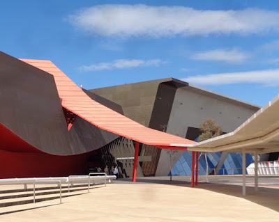
| Canberra: National Museum of Australia |
 |
| Canberra: National Museum of Australia |
 |
| Canberra: National Museum of Australia |
 |
| National Museum of Australia A History of the World in 100 Objects Object 20 Ramses II, Temple of Khum c.1280 BCE |
 |
| A History of the World in 100 Objects Object 101 Wireless LAN test and measurement System RF gets in somewhere! |
 |
| More RF! Canberra Deep Space Communication Complex: Dish DSS-43 (70-metre) |
 |
| No connection to RF. Paterson's curse is a pretty, innocent looking, flower invading Australia's grasslands |
 |
| Cooma cottage in Yass, near Canberra |
 |
| Queen Victoria in front of her building in Sydney |
 |
| Queen Victoria Building in Sydney |
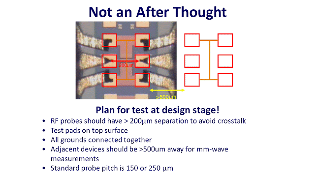
And now for RF Testing at Wafer level
Why?
•
Often
needed during development
•
Eg
to measure TSV performance or integrated passive components
•
Move
to advanced packaging solutions, eg WLCSP, has meant that measurements that
could previously be done at final package test are now needed at wafer level
•
Wafer
and die testing using a probe station is
fairly straightforward at low frequencies
•
Not
so easy at MHz and above
Cannot use conventional probes at > Mhz frequencies


