Monday 26 September 2016

RF Package Technology : Principles, Issues and Challenges in Penang

Weekend in Penang

 
Penang Street Food

Penang Street Food

Penang Street Food

More Street Food in Love Lane


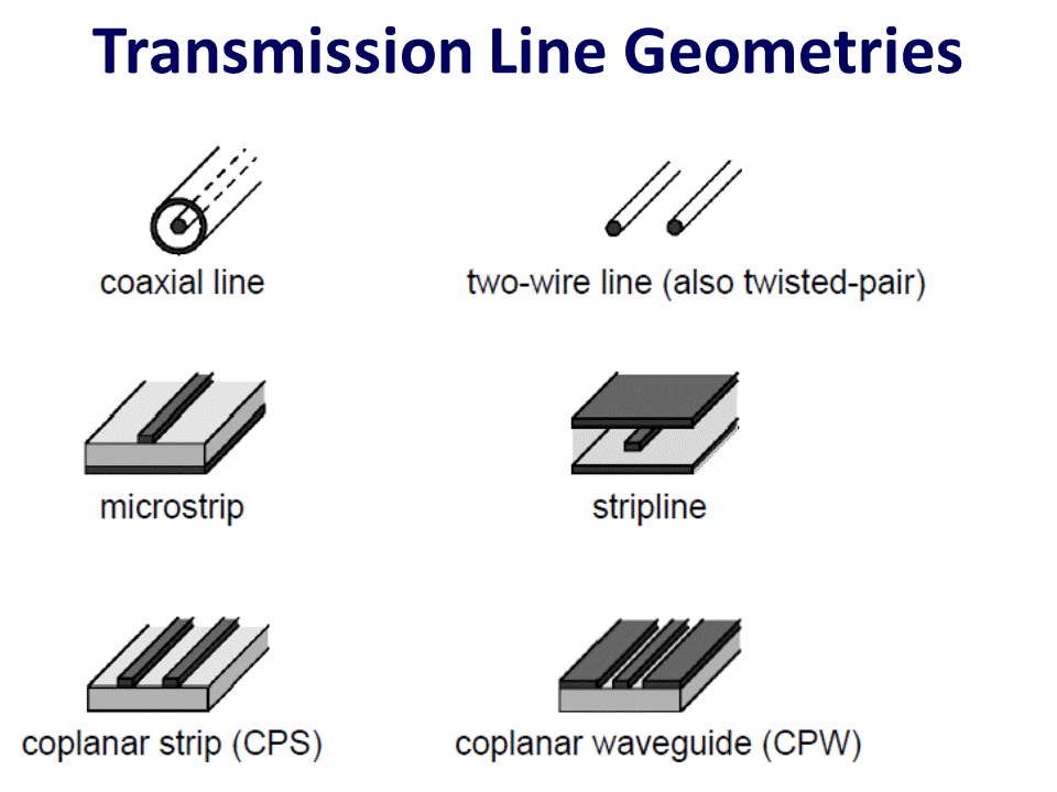
Just completed Day 1 of the course on RF Package Technology : Principles, Issues and Challenges

What sort of substrates should we be using for RF packages? There are plenty to choose from. Here  are some comparisons:


Technology
For
Against
Thin Film Ceramics
Wide range of substrate materials. Excellent line tolerance of ± 2.5 mm. Smooth high conductivity metals Traditional for high end mm wave applications. Circuits up to 100GHz
Hermetic
Expensive. Limited no of layers. Limited resistor ranges
Thick-Film Ceramics 
Wide range of substrate materials. Many decades of laser trimmed resistors  Hermetic. Lower cost than thin film
Poorer line tolerance ± 25 mm compared to thin film. Higher resistivity and roughness of metal layers. Limited no of layers
High Temperature Co-fired Ceramic (HTCC)
More layers than thick or thin film. Hermetic. Cheaper in volume production.
Shrinkage issues. Limited range of substrates.  Higher resistivity of metal layers. High tooling costs
Low Temperature Co-fired Ceramic (LTCC)
Better conductivity metal lines than HTCC. More layers than thick or thin film. Hermetic. Cheaper in volume production.
Shrinkage issues. Limited range of substrates. High tooling costs
Polymer Laminate
Low Cost. Standard SMT technology. Wide range of low permittivity substrates. Supports many metal layers. High conductivity smooth copper traces.
Poor linewidth tolerance ± 50 mm. Poor thermal conductivity. Not hermetic. Limited temperature range.

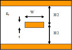
Just looking at ceramic substrates there are several to choose from:

Substrate
Applications
Properties
Alumina eg  99.6 %
Low to medium power  RF & microwave circuits
Permittivity=9.8
 Low cost  smooth, polished surface for fine lines 25 mm or better
Wide range of applications. Widely available
Quartz (SiO2)
Microwave & millimeter-wave circuits requiring extremely low loss or low
CTE
Permittivity=3.8.
Smooth, polished surface for fine lines 25 mm or better. Low loss tangent
Aluminium Nitride (AlN)
High-power RF & Microwave circuits using Silicon or GaAs ICs.  Optimal CTE match with Silicon devices
Permittivity=8.9 
Good thermal conductivity. Good TCE match to Si. Surface finish not as good as alumina or quartz
Beryllia (BeO)
High-power RF & Microwave circuits
Permittivity=6.7
Excellent thermal conductivity. Surface finish not as good as alumina or quartz. Dust is toxic.


Plymer laminates are popular due to low cots but the most widely sued, FR4 has some shortcoming at high frequency


Monday 19 September 2016

Kuala Lumpur and Transmission Lines

19th September 2016
Back and Forth between Malaysia and Singapore over the past couple of weeks

Petrona Towers

KL's Colonial Heritage


Finally sent off all my notes for the upcoming courses on  RF Package Technology : Principles, Issues and Challenges next week

Here’s a bit of a taster on transmission lines. 

There are plenty of transmission line geometries; for all except waveguide, they all have at least two conductors of which one is usually considered the ground. From an RF design perspective their most important parameter is their characteristic impedance Z0.


Waveguide is unusual in that the RF power travels inside a conducting tube, usually rectangular. 


For RF Packaging we can focus on three geometries. Each of them has its "for" and "against" points


Microstrip 

Commonest Transmission Line
Easy to fabricate
All active components can be mounted on top of PCB or substrate
Microstrip lines can couple to each other
Microstrip lines can radiate
Microstrip is dispersive, signals of different frequencies travel at slightly different speeds (Not usually a problem)

Stripline

Supports TEM Mode
Non dispersive (But may not be true at low frequencies where resistance of line has effect)
Non radiating
Excellent isolation between adjacent traces
Needs transition to microstrip to connect to components on board surface
More complex fabrication
Thicker board for given impedance and trace width
The two ground planes must be shorted together to prevent unwanted modes. Typically use row of vias on either side. Placement of these vias is critical

Co-planar Waveguide


Components can be mounted on board surface
Ground plane is on the board surface and close to signal line
Lower dispersion than  microstrip
Popular for wideband  systems  eg  optical  telecom  modules operating over bandwidths >10 GHz
Extremely high frequency response (100 GHz or more) since connecting to CPW does introduce parasitic discontinuities in the ground plane.
Excellent Isolation between traces
Does NOT support TEM Mode
Not supported by many CAD programs
No simple equation for Z0

Monday 5 September 2016

Ipoh and RF Packaging

A week in Ipoh, parts of which feel like they are still in the mid 20th century


Traditional Shophouses


1930’s Architecture

Oldest Mosque in Ipoh

5 Foot Way

Quiet Day at the Barber's
River Kinta dividing old and new towns


Working on upcoming course on Radio Frequency (RF) packaging.

Difficult to think that RF has only been around about 100 years.

It all started with Maxwell in 1864 but it was a slow start


It was nearly 30 years before anything of practical use came about.


These gentlemen with bowlers were  British Post Office engineers inspecting Guglielmo Marconi's wireless telegraphy (radio) equipment, during a demonstration on Flat Holm island, in 1897. This was the world's first demonstration of the transmission of radio signals over open sea, between Lavernock Point in South Wales and Flat Holm in the Bristol Channel, a distance of 3 miles. 

I grew up in Weston-super-Mare, within sight of Flat Holm, and despite doing physics at school and later working for Marconi Research in London and Essex, had no idea of Flat Holm's significance in radio history.  Nice to know you can now stay at a Marconi resort in  Lavernock Point. 
www.lavernockpoint.com

And, of course, it was Marconi's radio which played a significant and controversial role in the sinking of the   Titanic.

Just under 100 years ago in October 1916  Lee DeForest inaugurated music broadcasts in New York using vacuum valves, the development of which transformed radio into something close to what we know today. Guess he was the first radio disc jockey. 

Photo From Wikipedia


As the New York Sun reported“The technically inclined who wish to "listen in" should be informed that the "wave length" for hearing the music tonight will be 800 meters” (375kHz)

Which leads us right into RF Packaging! Note the wavelength and frequency: 800 meters” (375kHz)

We need to think about RF in packaging when the size  of the components is comparable with the wavelength of the signal. The usual rule of thumb is that we can treat circuit components as "lumped elements" if they are less than 1/10 the wavelength. For the 1916 music broadcast, that is 80 metres and we don't have any components that big! 


But modern computer chips and mobile phones work at GHz frequencies, about 10 000 times higher that the 1916 music broadcast.  The wavelength at 3GHz is about 10 cm so we need to be concerned at dimensions of about 1 cm, much smaller than a laptop or a phone. Life gets more complicated:
•“Wires” must be treated as transmission lines
•The skin effect increases the effective resistance of wires
•Coupling occurs between nearby components and wires
•Resistors, capacitors, inductors etc may no longer behave as lumped elements
•Wire bonds appear as series inductors
•Conducting housings may behave as enclosed cavity resonators

Watch this space for more or (plug, plug) come to one of my courses later this month in Penang and Manila.

26 & 27 September 2016 – Penang Workshop 
29 & 30 September 2016 - Manila Workshop o,

Further details from me at alastair@at-micro.com

or Atheena at atheena@lauresinternational.com


.